Entrepreneur, Engineer, Inventor, and Expert Witness
Barmak Mansoorian


BARMAK MANSOORIAN
INTRODUCTION
A semiconductor technologist driven by curiosity about how light becomes information. From being part of the invention of the CMOS Active Pixel Sensor at NASA JPL to my current work on SPADs photon-counting arrays at SWIRLabs, I’ve spent my career exploring how to push the boundaries of light detection. Here you’ll find my work, research, and consulting services in imaging innovation, semiconductor design, and expert witness analysis.






Projects
SPAD Photon-Counting Sensor
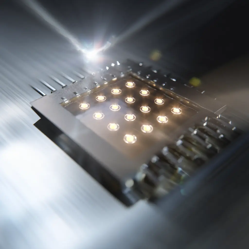
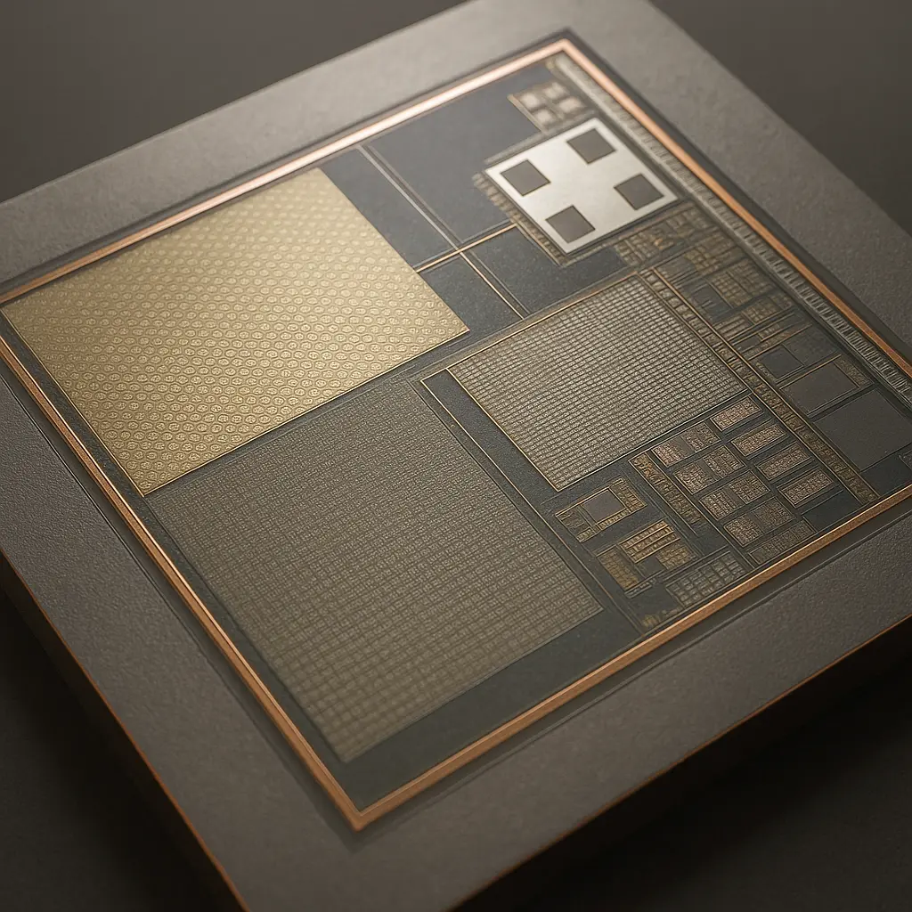
Development of a next-generation single-photon avalanche diode (SPAD) test chip integrating advanced 3D-stacked architectures, multiple imaging and spectroscopy modes, and sub-10 µm pitch arrays. The design demonstrates precision photon-counting and ultra-low-noise performance for emerging scientific and defense applications.
High-Speed CMOS Readout
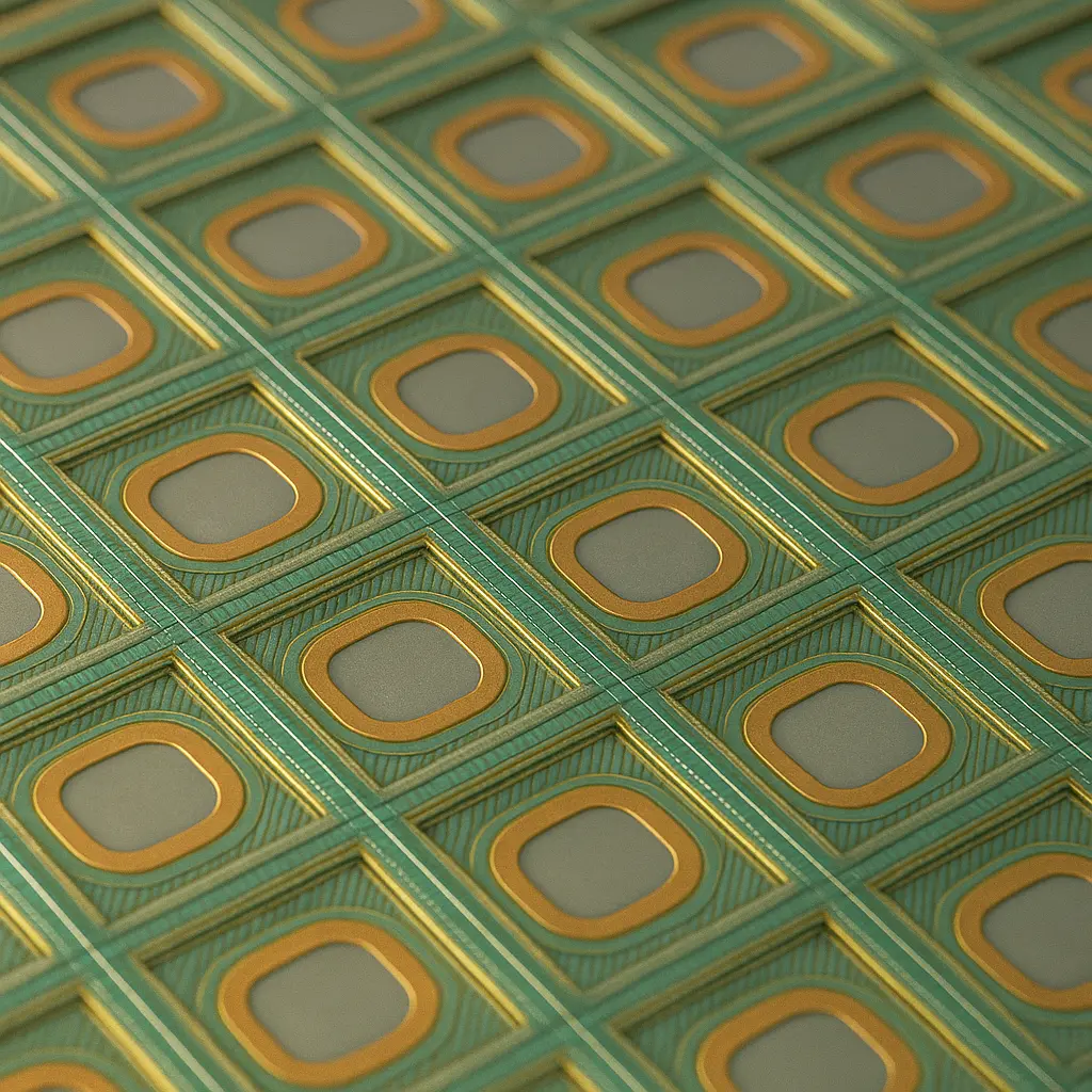
Architected and evaluated high-speed global-shutter CMOS image sensors with LOFIC (lateral overflow integration capacitor) and stacked ADC architectures for cinematic imaging. The work optimizes conversion gain, full-well capacity, and low-noise performance, achieving the balance of dynamic range and frame-rate needed for professional video systems.
Expert Witness | Imaging & Semiconductor Systems
Expert analysis and testimony in intellectual-property and technology-dispute cases involving image sensors, HDR algorithms, and semiconductor design. Draws on decades of experience in CMOS and SPAD imaging innovations, bridging technical rigor and legal clarity in complex patent and trade-secret matters.
